
Before I start, I should say a big thanks to Dave Jones and Chris Gammell for giving this project a shout-out on the excellent AmpHour weekly podcast. It sent my weekly reader stats up by a factor of 10! Cheers guys!
A number of people have contacted me about the LCR meter project. It is really good to hear from other people and find out what they think and has certainly given me some food for thought. I have been asked if I will be publishing the full schematics and making a PCB available. I will certainly be making the schematics and Gerbers available in a downloadable CAD file (probably Altium format). I may make a small number of prototype PCBs available if there are no bugs. I do not intend to sell any kits or complete products.
Not Design for Manufacture - Design for Me
It is worth me saying a few words about the general design of the LCR meter. Most designs have a target customer in mind. This might typically be a hobbyist kit constructor or a commercial product manufacturer. In this instance, the target customer is just me. This means that, in the first instance, I am designing around what is cheapest and most effective for myself. I have an FTDI USB module in my spares boxes, along with an AD5933, AD9834 DDS and PIC16LF1518.
If I were optimising this for minimum production cost, I would remove the DDS, multiplexers and PIC16. I would swap the controller for a PIC18 or ARM (anything cheap with USB capability and lots of I/O pins) and would replace the multiplexers with nice cheap 2-to-4, 3-to-8 or 4-to-16 logic decoders and MOSFETs acting as switches. Something along these lines:
 |
| Fig.1: Alternative inexpensive range select circuit |
The DDS would be replaced with a chain of dividers with some more MOSFETs to select the appropriate frequency division ratio. With sufficient free I/O pins, the binary decoders could probably be removed from the design too.
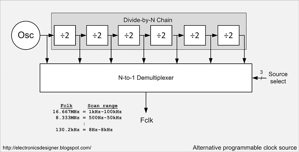 | |
| Fig.2: Alternative programmable clock source |
The most important thing I would add would be some protection against charged capacitors! I don’t measure big high voltage caps, but you can be sure that there would be users out there who would forget, and then blame me for not protecting their meter (and computer!). I guess I could add passive protection via some zeners on the sense connections, but I am not sure how big these would need to be to cope with a fairly meaty cap discharges whilst still protecting the meter.
An alternative would be a relay either isolating the meter, or acting as a crowbar across the measurement terminals. Relays do draw a relatively high amount of current though, reducing lifespan on battery powered devices, and can tend to oxidise over time, leading to intermittent contact.
If I were going to the extent of putting a relatively 32-bit ARM controller in there, that would open up the possibility of making it hand held, or at least a standalone portable. As it is, there will be a connector for a standard 4x20 LCD and a keypad, but they are there mostly for debugging. I have no requirement for a portable meter and that add another set of constraints that would push up both the development time and cost.
If I were going to the extent of putting a relatively 32-bit ARM controller in there, that would open up the possibility of making it hand held, or at least a standalone portable. As it is, there will be a connector for a standard 4x20 LCD and a keypad, but they are there mostly for debugging. I have no requirement for a portable meter and that add another set of constraints that would push up both the development time and cost.
Range Selection
You may recall from Part 1 that I am using two switched ranges to maximise the LCR meter's measurement range. The first of these controls the voltage across the Device Under Test (DUT), the second range selects the amount of gain generated by the I-V amplifier.
I selected the Analog Devices ADG706 16-channel analogue multiplexer for this task. 16 channels may seem somewhat over the top, but it is nice to have extra space to be able to experiment. I may well be using 10 or so gain settings in the receive amplifier anyway, so a 16 channel switch is ideal.
I selected the Analog Devices ADG706 16-channel analogue multiplexer for this task. 16 channels may seem somewhat over the top, but it is nice to have extra space to be able to experiment. I may well be using 10 or so gain settings in the receive amplifier anyway, so a 16 channel switch is ideal.
It is crucial that the multiplexer does not have a high “on” resistance, which would potentially affect the net value of the lowest feedback resistor (possibly as low as 100 Ohms). I have seen multiplexers with an “on” resistance as low as 0.5 Ohms, but these only appear to be 4 channels at best. The ADG706 has a usefully low “on” resistance of 2.5 Ohms which is pretty decent. Channel crosstalk capacitance and resistance figures seem to be sufficient too, but that will need testing to be sure.
Drive Amplifier
As it stands, the AD5933 is only designed to measure down to 1kOhms. At impedances below this, the drive amplifier cannot supply sufficient current. Whilst the AD5933 has a number of pre-set drive ranges, the manufacturer’s data sheet for the AD5933 advises the use of an external amplifier (actually acting as an active attenuator). They suggest using one of the following op-amps: AD8531, AD820, AD8641, AD8627. Comparing data, the AD8531 can drive the most current (+/- 250mA) and has the best capacitance driving ability (100nF @ 300kHz). Happily, it is also the cheapest one suggested.
100nF doesn’t seem a very high maximum capacitance, but in practise we don’t need the amplifier’s full performance. If we consider that a 100nF capacitor at 100kHz has an impedance of just 15.9 Ohms then we should be driving it at a lower peak-to-peak voltage, and at a lower frequency. Both of which greatly improve the chip's ability to drive capacitive loads beyond the headline spec. Although I do want to retain the ability to sweep as high a frequency range as possible, in order to detect potential resonances. This means that rather than driving the DUT at a standard 3V pk-pk we need to be looking at sub-mV level capability.
Stability at high capacitances and various drive frequencies needs to be tested. Unfortunately SPICE simulations aren't great at modelling this sort of thing.
Drive Offset
The AD5933 is a single-supply chip, and so generates a sinusoidal test signal which is biased by a DC offset. Normally this is not a problem as the receive amplifier simply subtracts the same amount. Curiously, the data sheet claims the output offset (for a 3.3V input) to be 1.48V, yet it shows the receive amplifier biasing the remote end of the DUT at Vdd/2 (1.65V). The recommended drive amplifier circuit also adds Vdd/2 to the existing offset. To confuse matters further, the AD5933 can also be programmed to drive at various pk-pk levels with a different offset. It may be easier to ignore this facility and rely on my own gain and offset control.
The design suggested in the data sheet clearly has the potential to generate a DC bias voltage (1.65V-1.48V=0.17V) which would manifest itself as an unwanted current in any inductor or resistor being measured. This would normally be calibrated out, but as we intend to measure relatively low values (and so generate small stimulus signals), the offset may swamp the intended signal and may generate a dangerously high current in low resistance DUTs. A trim pot would probably suffice if we were just using a fixed gain in the drive amplifier, but there is another possibility:
Programmable DC Bias Correction
Rather than using a fixed offset correction, how about using a small, low resolution DAC to set the null? This allows the unit to self-correct an offset which may drift according to gain and temperature, but it also allows us to superimpose the AC on top of a known DC bias if we so choose. The actual capacitance of many capacitors does change with voltage (many engineers are unaware of this) and it may prove useful to be able to test values with a bias voltage (or current in the case of inductors) even if it is only a modest +/- 1V or less.
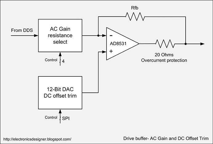 | |
| Fig.3: Drive Buffer - Programmable AC Gain and DC Offset Trim |
The 20 Ohms resistor output on the op-amp output is recommended in the application note. The AD8531 has a low impedance drive and is capable of sourcing and sinking 250mA. Accidentally going beyond this may result in damage, so a current limiting resistor is a sensible addition. It also helps to protect against the user attempting to test a charged capacitor.
Enclosure and Measurement Probes
Enclosure and Measurement Probes
What I haven’t yet decided is how I am going to connect the devices under test. This will in turn dictate how the meter is housed. A quick way of measuring surface mount devices might be to have a small PCB with a line etched down the middle, and a plastic mask over the top that holds the DUT in the correct position. That really means somehow obtaining a gold plated PCB though, unless I can find something to cannibalise for the job – maybe gold plated connector fingers. It all feels a bit too much like a rough-and-ready hack, which I want to avoid.Through-hole components will be tested via conventional test probes with standard 4mm banana connectors. Most test tweezers have standard banana plugs, which is useful, but I would rather have a hands-free test ability for small capacitances and inductances. Perhaps an external test fixture would be the best way.
That is pretty much where things are at right now. I have started schematic entry, but this new installation of Altium is being a pain. I really need a few hours together to concentrate on this beastie.
As ever, feel free to leave comments, it is always good to hear opinions and good ideas. See you in part three!
As ever, feel free to leave comments, it is always good to hear opinions and good ideas. See you in part three!
Hi Mike
ReplyDeleteWhen is part 3 coming?
I've got a hacked Rigol 1052E and a precision gold (£50 pound DMM), would these bits of kit be good enough for calibration for this project or (I am assuming) do I need a much more accurate DMM to calibrate.
Thanks Richard
Ps I'll be up for one of those PCB's if there is one spare ;)
Hi Richard.
ReplyDeleteI haven't used this chip before, so I don't know quite how it will behave in the real world. In theory it should be possible to calibrate it with a short circuit, open circuit and a handful of close tolerance components. The next step is to get the schematic captured and a PCB generated. I'm fairly busy at the moment though, so it may take some time :(
Mike
Mike,
ReplyDeleteJust wondering if you have progressed this project any further?
- John
Yep, I have done quite a bit of development to the LCR meter. Unfortunately family and work commitments have meant that I just haven't got it to the state where I have anything significant to show. I'm not sure people would be interested in pages and pages of scribbles and ponderings. The next step is schematic capture and PCB design, and I really need a day or two to devote to that.
ReplyDelete